Moore's Law was an economic pattern, not a law of nature
Transistors are running out of road because making them smaller no longer guarantees a cheaper, faster and more efficient computer. That is what people mean when they ask whether Moore's Law is ending. The limit is not one solid wall. It is a tightening knot of leakage, heat, wiring delay, manufacturing difficulty and cost. Once those limits are clear, the technologies that come after traditional transistor scaling make sense: new transistor shapes, stacked chips, chiplets, specialized processors and better software.
In 1965, Fairchild Semiconductor research director Gordon Moore noticed that manufacturers had been putting more components on each integrated circuit at a rapid, regular pace. His original paper projected an annual doubling for about a decade. In 1975, he revised the pace to roughly a doubling every two years. The familiar version of Moore's Law is therefore an observation and an industry target: transistor counts on economically produced chips tend to double about every two years.
The economical transistor count on an integrated circuit tends to grow exponentially over time.
Every computer must become twice as fast every two years. That was never the law.
The distinction matters. More transistors can hold more memory, perform more arithmetic at once, or run a new kind of accelerator. They do not automatically make one sequence of instructions run twice as fast. The doubling pattern is exponential, so the mathematics of logarithms is the right tool for finding doubling times and comparing growth rates.
If a design begins with 1 million transistors and the doubling time is two years, then after six years it has transistors.
For decades, shrinking a transistor helped several goals at once. A smaller device occupied less area, switched faster, needed less energy per switch and cost less when a wafer yielded many working chips. This bundle of benefits made Moore's pattern feel automatic. It was actually the result of repeated inventions in optics, chemistry, materials, device design and factory control.
A transistor is a gate controlling a current
The logic transistor used in processors is a microscopic electrical switch. A voltage on its gate changes the conductivity of a channel between two terminals called the source and drain. Circuits interpret the resulting low and high voltages as binary states.
Most digital chips use metal oxide semiconductor field-effect transistors, usually shortened to MOSFETs. The gate is separated from the channel by an insulating layer. Apply a suitable gate voltage, and an electric field gathers charge carriers in the channel so current can flow. Remove that voltage, and the channel should stop conducting. No moving mechanical part is required.
Logic gates combine transistors to compute operations such as NOT, AND and OR. Larger arrangements form adders, registers, memory controllers and processor cores. A chip is therefore not a bag of isolated switches. It is a timed electrical system whose useful work depends on transistors, wires, memory and power delivery all behaving together.
Shrinking helped because a shorter channel gave charge carriers less distance to travel, while smaller capacitances took less charge to change voltage. Engineers could raise the clock frequency and still keep power under control. This favorable relationship is associated with Dennard scaling, described in a 1974 paper led by IBM researcher Robert Dennard.
Those two trends are easy to confuse because they operated together for years. Moore's Law concerns component density and cost. Dennard scaling concerns how voltage, current and power behave as dimensions shrink. Transistor counts can keep rising after the old power relationship fails, but designers must then decide which transistors can be active and what jobs they should do.
The power bargain broke before transistor counts stopped rising
Smaller transistors once allowed lower supply voltages to offset the power used by having more switches. Voltage could not keep falling at the same rate, because a smaller gap between on and off voltages makes logic unreliable and worsens leakage. Power density then became a design limit.
Charging and discharging the tiny capacitances in a chip consumes dynamic power. A useful simplified relation is:
Here is switching activity, is capacitance, is voltage and is clock frequency. Cutting voltage from 0.8 V to 0.7 V changes the voltage term by , about a 23% reduction if the other terms stay fixed.
The square on voltage made voltage reduction exceptionally valuable. But a transistor must clearly distinguish an on state from an off state despite manufacturing variation, electrical noise and thermal motion. Lowering voltage too far slows switching or causes errors. Meanwhile, an off transistor is not perfectly off, so billions of supposedly idle devices can still leak current and produce heat.
A phone starts a demanding game. Its processor briefly raises clock speed, power use climbs and the chip warms. The cooling system cannot remove unlimited heat, so control circuits reduce frequency. The chip contains plenty of transistors, but the heat budget decides how many can work hard at once.
This is why desktop processor clock speeds stopped climbing at their earlier pace and multicore designs became standard. More cores can increase throughput when work can be split into independent pieces. They cannot make every program proportionally faster, because some steps depend on earlier results. Scheduling, communication and memory access also consume time.
Engineers sometimes call the unused portion of a chip dark silicon. The phrase does not mean that the transistors are broken. It means power and cooling limits prevent every available circuit from operating at maximum activity simultaneously. Designers may switch blocks on only for the tasks they handle well.
Small channels weaken the gate's control
A transistor fails as an ideal switch when its channel becomes so short that the drain and source strongly influence it. The gate then has less exclusive control, leakage increases, and quantum tunnelling makes very thin barriers less effective. Smaller geometry produces new electrical behavior.
In a large planar MOSFET, the gate sits above a flat channel. As the source and drain move closer, their electric fields reach farther into that channel. The drain can lower the energy barrier that is meant to block current when the device is off. Engineers call the family of resulting problems short-channel effects.
The gate insulator creates another constraint. A thinner layer gives the gate stronger electrostatic control, but electrons have a probability of tunnelling through a sufficiently thin barrier. Manufacturers responded by replacing silicon dioxide with materials that have a higher dielectric constant, called high-k dielectrics. A physically thicker high-k layer can provide strong electrical coupling with less direct gate leakage.
These quantities describe different things. The lithography wavelength is not the minimum printed feature because optical systems, masks, photoresist chemistry and computational pattern correction work together. The physical channel length is not the marketing name of a process. The doubling interval is an industry trend, not a timer built into silicon.
Atomic scale variation also matters. A small difference in an edge, a material layer or the position of an impurity can change one tiny device more than it would change a large one. Fabrication must repeat many processing steps across a wafer while keeping enough chips within specification. A clever laboratory transistor is only the beginning; a useful process must manufacture dense circuits with acceptable yield.
The node name is not a transistor measurement
Names such as 7 nm, 5 nm and 3 nm identify generations of manufacturing technology, not one universal dimension on the chip. Different companies use different naming systems, so equal node numbers do not prove equal transistor density, speed, power or cost.
Earlier process names were more closely connected to a physical feature such as gate length. Over time, transistor geometry became three-dimensional and the relevant pitches and widths stopped shrinking in lockstep. A single number could no longer describe the gate, wiring, memory cells and logic density. Commercial naming continued because buyers still needed labels for process families.
A 3 nm process does not contain a single defining part that is exactly 3 nm long. Treat the label as a generation name, then examine the measurements and products that matter for the comparison.
This also explains why declaring an exact date for the death of Moore's Law is slippery. Density may rise through smaller standard cells or through several dies in one package. Announcements may count a chip, a die, a package or one circuit type. The original economic idea concerns useful complexity at manageable cost.
New geometry is extending the transistor's useful life
Engineers have not stopped shrinking transistors. They have changed the switch's shape so the gate controls more sides of the channel, changed the materials around it, and rearranged power wires. Each move buys electrostatic control or usable area, but also adds manufacturing steps and design constraints.
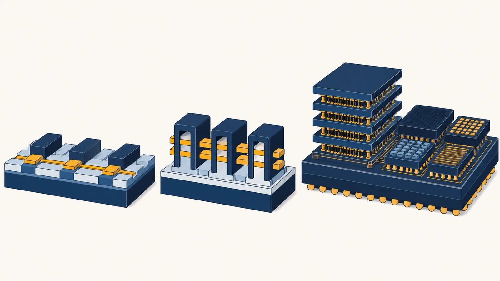
The planar transistor gave way at advanced nodes to the FinFET. In a FinFET, the channel rises like a narrow fin and the gate wraps around three sides. Intel put its 22 nm tri-gate version into high-volume production in 2012. More contact between gate and channel improves control and reduces unwanted current.
Gate-all-around designs take the idea farther. The channel becomes one or more horizontal nanosheets or nanowires surrounded by gate material. Engineers can choose sheet dimensions to balance current, capacitance and layout. The wraparound gate better controls a short channel, although building uniform stacked sheets and contacts is demanding.
John Bardeen and Walter Brattain demonstrated the point-contact transistor at Bell Labs, with William Shockley leading the solid-state research group.
Gordon Moore plotted component counts and projected rapid growth in the complexity of economical integrated circuits.
Robert Dennard and colleagues explained how MOSFET dimensions, voltage and current could scale together while controlling power density.
Intel's 22 nm process used three-dimensional tri-gate transistors, moving leading logic away from a flat channel.
That sequence belongs to the wider history of inventions and industry, because physics alone did not decide which ideas reached mass production. Research institutions, factories, supply chains and trained workers also shaped the result.
Backside power delivery tackles a different obstruction. Conventional chips route both signals and power through metal layers above the transistors. Moving some power connections to the rear of the wafer can reduce congestion and voltage loss, leaving front-side wiring more room for signals. It does not repair a leaky channel, but it can improve the complete circuit.
The wires are becoming as limiting as the switches
A computation needs signals to travel between transistors and data to move between logic and memory. Thin, crowded interconnects have resistance and capacitance, which create delay and consume energy. A faster transistor cannot help while it waits for operands to arrive through the wiring.
Long on-chip wires do not shrink into perfect conductors. Narrower metal lines generally have greater resistance, and nearby lines couple capacitively. Contacts and vias occupy area. Repeating a signal over distance takes additional circuits and power. This is why a process roadmap must cover interconnects, not only the transistor channel.
How can each transistor become smaller and switch faster?
Where should computing and memory sit so that less data must travel?
Chiplets answer part of that system question. Instead of manufacturing one enormous die with every function, a designer can join smaller dies inside one package. A processor die, input and output die, cache die and accelerator can use processes suited to their jobs. Smaller dies may also avoid throwing away a whole large chip because of one manufacturing defect.
Packaging is not free. Links between dies use energy and introduce delay. Heat must escape from a denser three-dimensional assembly. The engineering target shifts from the best isolated transistor to the best complete package.
Vertical stacking shortens some connections and creates more usable device area without demanding the same shrink in every horizontal feature. Memory dies are already stacked in several product classes, while research roadmaps extend stacking toward logic. The 2024 IEEE International Roadmap for Devices and Systems projects that three-dimensional integration becomes necessary as ordinary two-dimensional geometry runs out of placement room.
Computing gains are moving into architecture and software
After easy scaling, performance comes increasingly from doing less work, moving less data and matching hardware to the calculation. Parallel cores, vector units, graphics processors and dedicated accelerators can be much more efficient than a general processor, but only for workloads shaped to use them.
A graphics processor runs many similar operations at once. A machine-learning accelerator may devote large areas to matrix multiplication and nearby memory. A video encoder implements a narrow family of transformations directly in hardware. Specialization removes general-purpose machinery, which can save time and energy, but the specialized block is less useful when the task changes.
Measure whether time and energy go into arithmetic, memory access, communication or waiting. A faster multiplier cannot repair a memory bottleneck.
Split independent operations across cores or vector lanes while preserving dependencies that determine the correct result.
Keep reused data nearby and use only as much numerical precision as the application requires. Moving a value can cost more energy than operating on it.
Acceleration pays when the workload is common and stable enough to justify silicon area, programming effort and data conversion.
Software therefore becomes part of the scaling story. A better algorithm can remove work rather than execute the same work faster. Compilers can arrange instructions for vector units and move data through memory hierarchies. Programmers can trade precision for speed where errors remain acceptable. None of these gains arrives uniformly across every program.
There is also a resource question. Fabricating chips requires energy, water, processed minerals and an international production network. Studying how societies classify and manage finite resources helps separate the physical supply of a material from the economic conditions that make it available. More efficient computing can lower energy per task, yet cheaper computation can also increase the number of tasks demanded.
That rebound makes efficiency a social issue as well as an engineering one. Electricity prices may not include all damage caused by pollution, while a company buying computing power does not make every affected community part of the transaction. The economics of costs that markets fail to capture explains why efficiency improvements and environmental rules may need to work together.
Progress after Moore's Law will be real, uneven and measurable
There is no single replacement law that promises every computer will improve on schedule. Progress will come from combined gains in devices, wiring, packaging, architecture, algorithms and manufacturing. Each application will improve at a different rate because each has a different limiting resource.
For a scientific model, the limiting resource may be memory bandwidth. For a hearing aid, it may be battery energy and response time. For an industrial controller, reliability may matter more than peak arithmetic speed. Asking what is being measured prevents a density claim from masquerading as a universal performance claim.
The takeaway: Transistors are not about to disappear, and Moore's Law will not stop on one date. The old package deal is separating. More transistors, faster switching, lower energy and lower cost now require different solutions, so future gains must be judged at the level of the whole system and the task it performs.
The most useful question is no longer simply how many transistors fit on a chip. Ask how much correct work a system completes for its money, energy, time and material cost. That test recognizes the physical limits without treating them as the end of invention.